
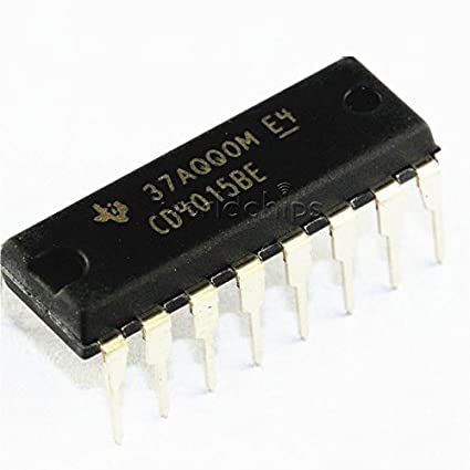
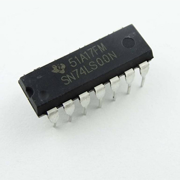
CD4015BE
Price:
RWF 1,000Added to Cart!
Need help or have questions about this product?
Contact STS Support →Product Description
The CD4015BE is a versatile and reliable integrated circuit that consists of two identical, independent, 4-stage serial-input/parallel-output registers. Each register has independent CLOCK and RESET inputs as well as a single serial DATA input, making it an ideal component for a wide range of applications. With its compact design and robust functionality, the CD4015BE is perfect for use in Arduino projects, breadboard prototypes, and other electronic circuits that require efficient data processing and storage.
Specifications:
- Two independent 4-stage serial-input/parallel-output registers
- Independent CLOCK and RESET inputs for each register
- Single serial DATA input for each register
- Compatible with Arduino and other microcontroller platforms
- Can be used with ULN2003 Driver Board for enhanced functionality
Applications:
- Arduino projects and prototypes
- Breadboard circuits and electronic prototypes
- Pump control and automation systems
- Servo motor control and robotics projects
- Other electronic circuits that require serial-to-parallel data conversion
Why Buy from SoftTech Supply?
- Genuine electronic components from trusted suppliers
- Competitive prices on Arduino, Raspberry Pi, sensors & more
- Fast delivery across Kigali and Rwanda
- Expert technical support and project consultation
- Easy returns and quality guarantee
Related Products
TDA0161 Metal body proximity detector IC
SG3524N Pulse-Width Modulator
PT2262 DIP 18 Remote control Encoder
Buy CD4015BE at STS - Kigali, Rwanda
CD4015BE is available at SoftTech Supply, your trusted electronics shop in Kigali, Rwanda. We stock genuine electronic components including Arduino boards, Raspberry Pi, ESP32, ESP8266, various sensors, motors, displays, and thousands of other components for your IoT, embedded systems, and electronics projects. Visit our shop or order online for fast delivery across Rwanda. Need help selecting components or implementing your project? Contact STS for expert technical support and consultation.